GPIO Interface Electrical Requirements
Applicable to R1.0 hardware only
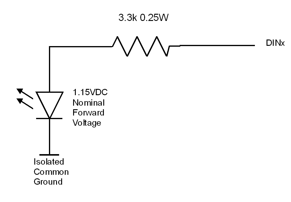
External Inputs 0-7:
These signals are optically isolated from the rest of the system. The External Input Ground pin is also isolated from the rest of the CDP unit. Current draw of the input is approximately 500 uA for a 3VDC input, increasing to 8.5 mA for a 30 VDC input. In order to see a “1” on a Din pin, you need to supply a voltage between 3VDC and 30VDC to turn on the optoisolator input.
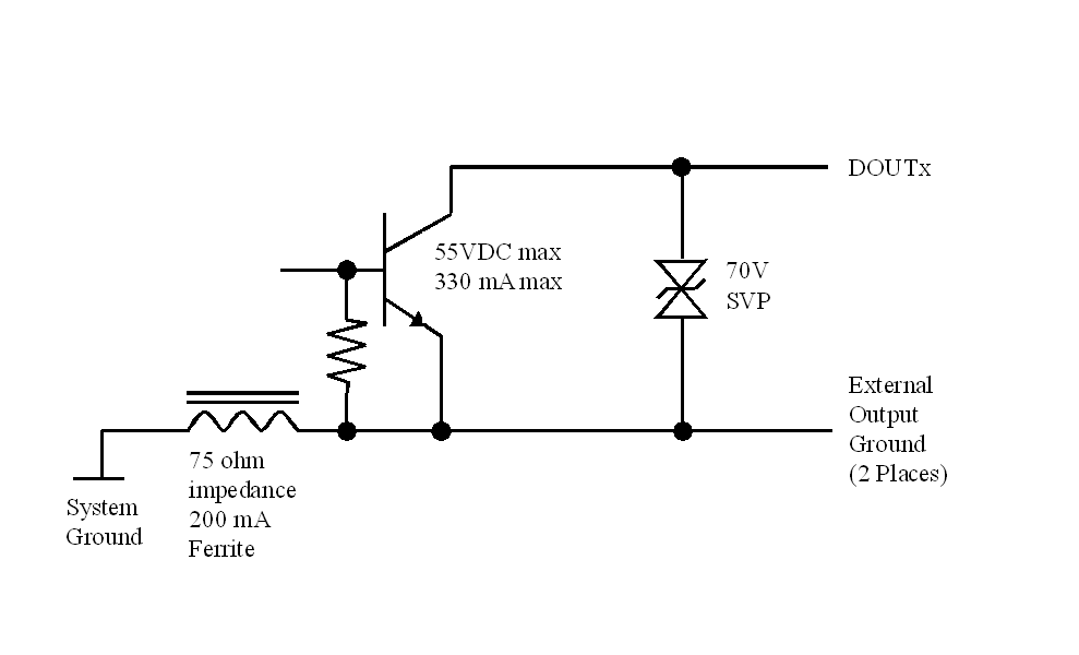
External Outputs 0-7:
These signals are open collector with maximum working voltage Of 55VDC and maximum current draw of 300mA. These signals share a common ground with the CDP, and cannot be used on isolated signals. If an output is used as an “digital” signal, an external pull up resistor is required for proper operation. If an output is being used to drive an inductive load, such as a relay, a clipping diode is recommended to protect the output circuitry from inductive spikes.
Equivalent circuit:
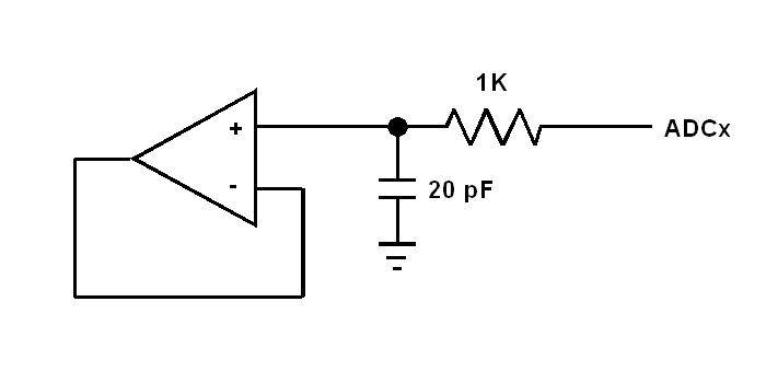
Analog Inputs 0-4:
These signals are analog inputs fed through an operation amplifier buffer to a 10 bit Analog to Digital converter. The inputs are multiplex, so only one voltage is converted per system call. The input is scaled to accept a 0-5VDC input.
Debug Serial:
The Debug serial pins are a standard RS232 signal levels and can be connected to any RS232 interface. The serial interface signals are labeled as a DTE device so Debug_RX connects to the TXD pin of connecting terminal and Debug_TX would be connected to the RXD pin.
|
D9 Pin |
RS232 Signal |
CDP Debug Serial |
CDP I/O Pin |
| 1 | DCD | N/C | – |
| 2 | RX | Debug_TX | 31 |
| 3 | TX | Debug_RX | 30 |
| 4 | DTR | N/C | – |
| 5 | GND | Digital Ground | 36 |
| 6 | DSR | N/C | – |
| 7 | RTS | N/C | – |
| 8 | CTS | N/C | – |
| 9 | RI | N/C | – |
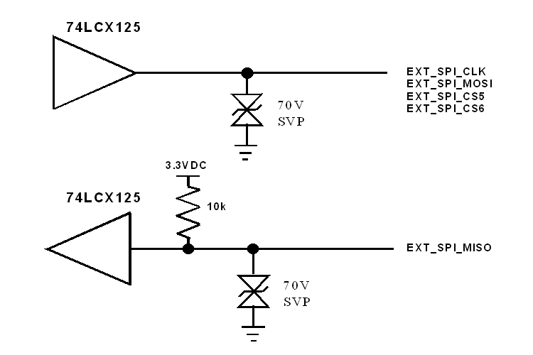
External SPI Bus:
The external SPI bus is shared with the internal SPI bus. The External SPI bus is fully buffered and only active when an external device is selected (CS5 or CS6). The buffers are limited to 3.3V so only devices that are 3.3V compatible can be used on the external SPI bus. Maximum clock speed of the bus is limited by the external signal path.
External I2C Bus:
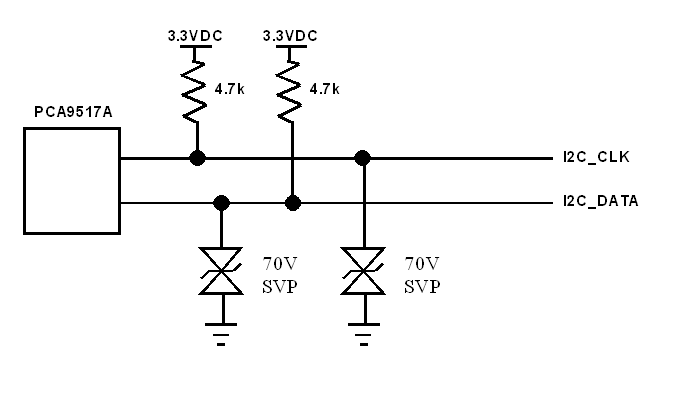
The external I2C bus is shared with the internal I2C bus. The External I2C bus is fully buffered. The buffers are limited to 3.3V so only devices that are 3.3V compatible can be used on the external SPI bus. Maximum clock speed of the bus is limited by the external signal path. The buffer can handle up to 400 pF of capacitance load and can operate at either the Standard (100 kHz) or Fast (400 kHz) clock rate. Both the I2C_CLK and I2C_DATA line are open collector and have an internal 4.7K pull-up to 3.3VDC. To improve perfomance of the bus, additional 4.7K pull up to 3.3 VDC can be used on each signal at the end of the cable.
GPS PPS (Pulse Per Second):
The GPS Pulse Per Second signal is a buffered 3.3VDC output. This pin outputs a 1 msec pulse every second, after the GSP has locked and received a position fix. This output can sink or source up to 24 mA of current at 3.3VDC.
